ASML's Lithography Technology Roadmap: From DUV to Hyper-NA and the Future of Chip Manufacturing
ASML dominates the chipmaking lithography market with its deep ultraviolet (DUV) and extreme ultraviolet (EUV) systems. In 2025, the company shipped 48 EUV and 131 immersion DUV tools, generating €32.7 billion in revenue and ending the year with a €38.8 billion order backlog. This Q&A breaks down ASML's technology evolution—from established DUV to next-generation High-NA, Hyper-NA, and concepts beyond—explaining how these systems enable ever-smaller transistors.
1. What Are the Main Types of Lithography Systems ASML Currently Offers?
ASML's portfolio centers on two core technologies: DUV (deep ultraviolet) and EUV (extreme ultraviolet). DUV machines use 193 nm wavelength light and are further divided into dry and immersion variants. Immersion DUV systems, which use water between the lens and wafer, achieve higher resolution and are widely used for manufacturing advanced logic and memory chips. In 2025, ASML shipped 131 of these immersion tools. EUV systems, using 13.5 nm wavelength light, enable the patterning of tiny features below 7 nm (e.g., 5 nm, 3 nm nodes). ASML delivered 48 EUV systems in 2025. These two families—DUV for mature and mid-range nodes, EUV for leading-edge—form the backbone of current semiconductor fabrication.
2. How Do DUV and EUV Technologies Differ in Chipmaking?
The primary difference lies in wavelength and resolution. DUV's 193 nm wavelength limits the smallest features to roughly 38 nm with immersion techniques, while EUV's 13.5 nm wavelength can resolve features below 10 nm, down to 7 nm and smaller. DUV systems rely on multiple patterning steps (e.g., quad patterning) to achieve these sizes, making them increasingly complex and costly. EUV systems, by contrast, use single-patterning for many critical layers, reducing process steps and improving throughput for leading-edge chips. However, EUV tools are significantly more expensive (€150+ million per system vs. €30–60 million for DUV) and require a vacuum environment. In 2025, ASML's revenue mix reflects this: EUV systems contributed a larger share of total revenue despite fewer shipments, underscoring their value in advanced node production.
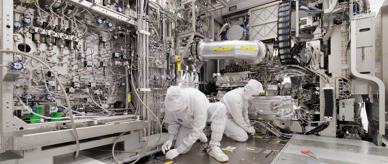
3. What Are Low-NA and High-NA EUV Lithography?
Low-NA EUV refers to the current generation with a numerical aperture of 0.33, suitable for 7 nm and 5 nm nodes. High-NA (high numerical aperture) EUV systems, with a NA of 0.55, are designed for 3 nm and 2 nm nodes and beyond. The higher NA allows finer resolution—down to about 8 nm features—enabling smaller, more power-efficient transistors. ASML's first High-NA system, the EXE:5000, is in production since 2024. High-NA machines are physically larger, require new mirrors, and cost over €400 million each. They reduce the need for multiple pattern steps, lowering overall chip-making costs at advanced nodes. ASML is ramping High-NA production to meet demand from leading-edge foundries like TSMC and Intel. The capacity for these systems is critical to the industry's ability to continue Moore's Law scaling.
4. What Is Hyper-NA and What Comes After EUV?
Hyper-NA is a proposed extension of EUV with a numerical aperture above 0.55 (e.g., 0.77 or 0.85). It would push resolution below 7 nm, potentially reaching 0.5 nm features, but faces enormous technical hurdles: new reflective optics with extreme precision, higher vacuum demands, and greater power sources. ASML has not yet announced a specific Hyper-NA product; it remains a research path for the 2030s. Beyond EUV, the industry is exploring multi-beam and nanoimprint techniques, as well as soft X-ray lithography. However, no clear successor has emerged. ASML's roadmap includes continued refinement of High-NA for the next decade, with Hyper-NA as a possible bridge to post-EUV solutions. The timeline depends on semiconductor industry demand for even smaller nodes.
5. What Do ASML's 2025 Shipment Numbers Tell Us About Market Trends?
In 2025, ASML shipped 48 EUV systems and 131 immersion DUV tools, generating €32.7 billion in revenue. The €38.8 billion order backlog indicates strong future demand, particularly for EUV tools as chipmakers race to build 3 nm and 2 nm capacity. The high number of DUV shipments (more than double EUV) reflects continued reliance on DUV for mature nodes, memory chips, and less advanced logic. However, the revenue share shows EUV systems command much higher selling prices. Growth in 2025 was driven by investments from TSMC, Samsung, and Intel, along with expanding chip demand for AI and computing. The backlog suggests that while DUV still moves large volumes, the profitability and future focus are shifting to EUV and, soon, High-NA systems.
6. How Does ASML's Order Backlog Reflect Chip Industry Outlook?
ASML ended 2025 with a €38.8 billion order backlog, up from previous years. This indicates chipmakers are committing to long-term lithography capacity, especially for EUV and High-NA tools. The backlog includes orders from leading-edge foundries, memory manufacturers, and chipmakers expanding capacity in regions like the US, Europe, and Asia. Notably, the backlog growth aligns with the semiconductor industry's push for smaller nodes (3 nm, 2 nm) to power AI accelerators, high-performance computing, and mobile devices. It also signals that supply constraints for advanced chips are being addressed. However, the backlog also implies delivery lead times of several years for some systems, potentially slowing the pace of technology adoption. Overall, the strong backlog confirms healthy demand and a bullish outlook for advanced lithography through the late 2020s.
Related Discussions